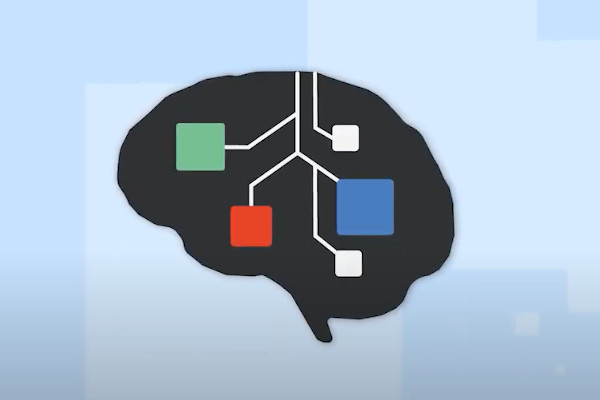
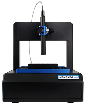
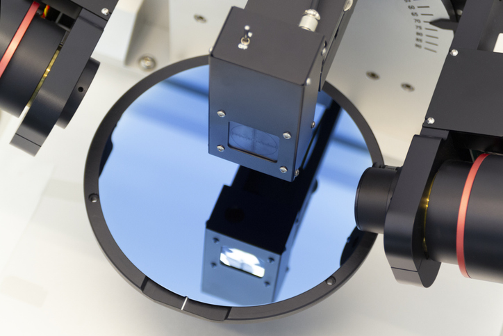
Insights
Take a deeper dive into our product range and the associated industries and technologies
Want to learn more?
Please browse our range of articles or go ahead and contact us if you would like to talk more.
May 28, 2025
Surface profilometry is a critical tool in material science, which allows researchers and manufacturers to assess the topography of a material with exceptional precision. From nanoscale roughness to large-scale surface features, profilometry provides insights that are essential for material characterisation and quality control. We explain more in our latest insights blog.
May 20, 2025
From the silicon in microchips to the gallium nitride in high-efficiency LEDs, semiconductor materials are at the heart of innovation. In our latest insights article, we delve deeper into semiconductors, outlining what they are and how they are used.
April 3, 2025
Thin films are everywhere. They are a layer of material that ranges from fractions of a nanometre to a few micrometres in thickness. They can be found in everything from optical devices to electrical components to protective coatings – wherever a very thin layer of material is needed for a specific function.
Contact us
We’d love to hear from you
We’re here and ready to provide information and answers to your questions
Policy Information
©Mi-Net 2023. All Rights Reserved.
Website by Fifteen.co.uk