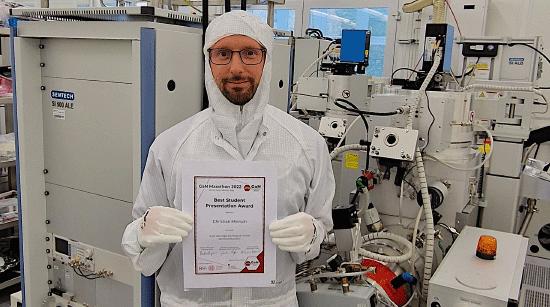
At the recent GaN Marathon 2022 held in Venice Italy, Christian Miersch, PhD student at Fraunhofer IISB, received a “Best Student Presentation Award” based on his talk “Low Damage Etching of Nitride Semiconductors”. The GaN Marathon is a workshop designed to present research and the latest results for gallium nitride in microelectronics and optoelectronics. Christian’s talk explained the recessing and annealing conditions of AlGaN/GaN heterostructure to achieve an ohmic contact (or a low resistant ohmic contact). This was achieved by recess atomic layer etching into the AlGaN barrier of HEMT (high electron mobility transistor) structures. Recessing atomic layer etching of the AlGaN layer plays a critical role in GaN device properties, as it can lead to surface state modifications, lattice order and species contamination. The key goals were reducing contamination, thermal stress, damage and degradation of the substrate material, as well as achieving a low surface roughness. The SENTECH cluster tool combining the plasma process plasma enhanced atomic layer etching, ICPECVD, and PEALD tools successfully realised the low damage etching of GaN devices and delivered some promising results, as presented by Christian Miersch. Christian Miersch is a PhD student in Fraunhofer IISB’s Spectroscopy and Test Devices Group within the Materials Department, located in the Fraunhofer Technology Centre High-Performance Materials THM in Freiberg, a research and transfer platform of Fraunhofer IKTS and Fraunhofer IISB.
A huge congratulation from the team at Mi-Net and SENTECH and we look forward to supporting many more such successful research collaborations in the future.
For more information about the tools used by Christian, please visit our pages for Thin Film Processing Technology.