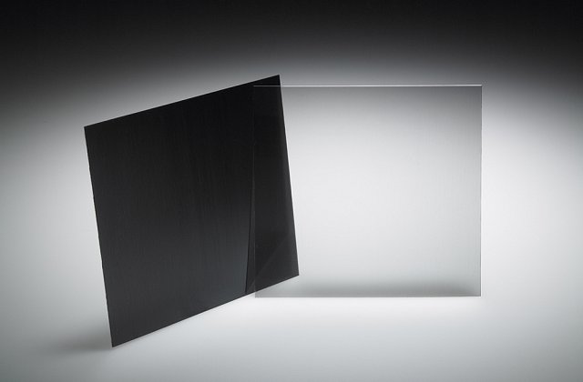
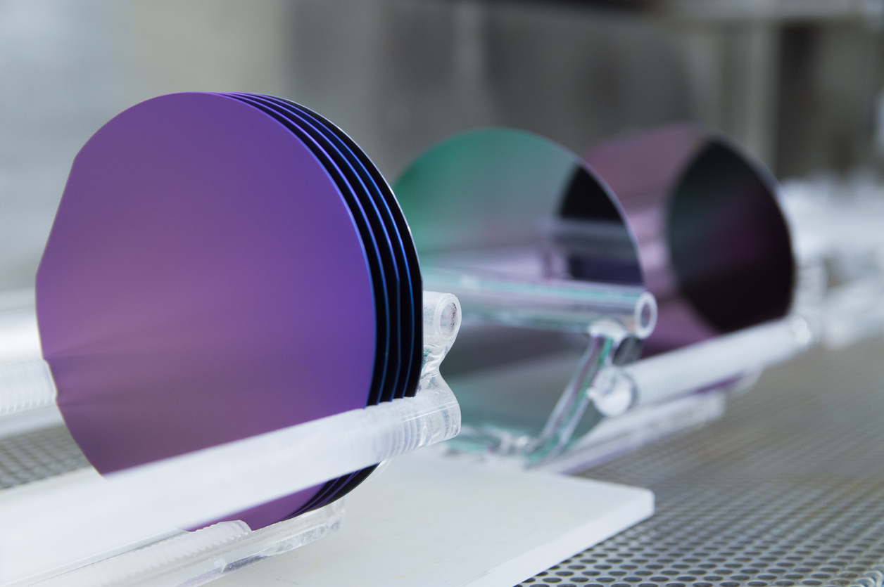
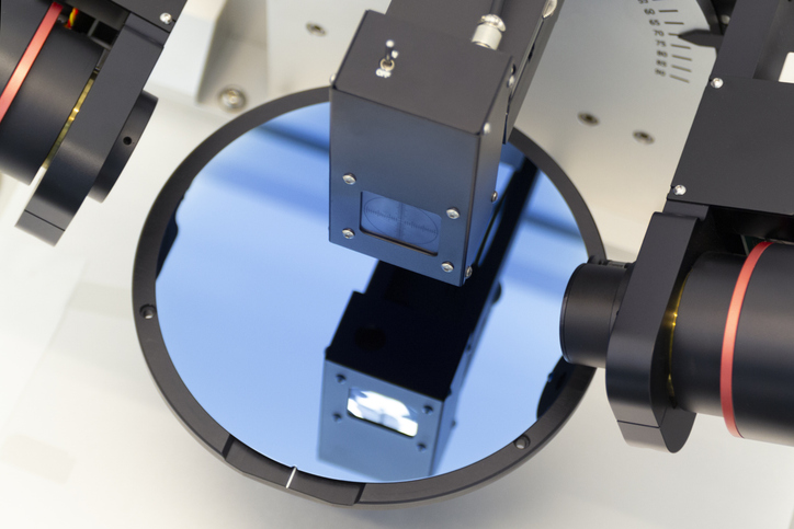
Silicon carbide (SiC) has emerged as one of the most important wide-bandgap materials in modern semiconductor technology, enabling a new generation of high-power, high-voltage and high-temperature devices. Once limited to niche applications, SiC is now a cornerstone material for power electronics used in electric vehicles, renewable energy systems, industrial motor drives, aerospace and high-voltage power conversion.
What makes silicon carbide attractive is its combination of exceptional physical and electronic properties. Compared with conventional silicon, SiC offers a much wider bandgap, significantly higher breakdown electric field, superior thermal conductivity, and excellent chemical stability. These characteristics allow devices to operate at higher voltages, higher switching frequencies and elevated temperatures, while reducing conduction and switching losses. The result is smaller, lighter and more energy-efficient power systems which offer a compelling advantage as efficiency and power density become critical design constraints.
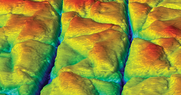
However, these same properties that make SiC so powerful also make it challenging to work with. Silicon carbide is extremely hard, chemically inert and difficult to process using traditional silicon semiconductor techniques. Crystal growth, wafer uniformity, defect density, and material stress remain significant technical hurdles. Fabrication steps such as wafer polishing, etching and high-temperature processing demand specialised equipment, robust materials and tightly controlled processes. Yield management and cost control continue to be central challenges as the industry scales production.
Despite these difficulties, ongoing advances in crystal growth, wafer quality, device design and manufacturing infrastructure are rapidly maturing the SiC ecosystem. As performance demands continue to outpace the limits of silicon, silicon carbide is increasingly viewed not as an alternative, but as a necessary material for next-generation semiconductor devices.
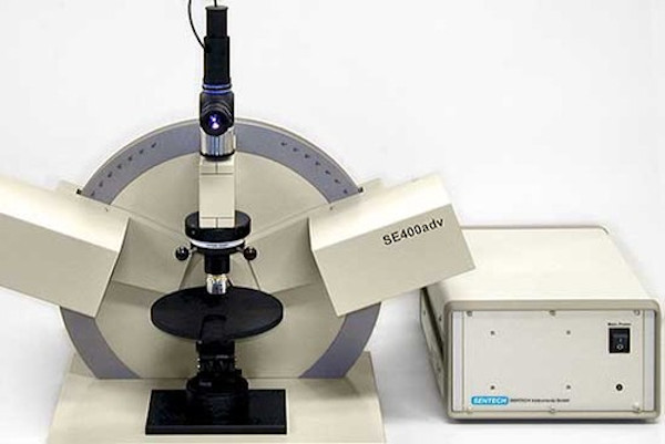
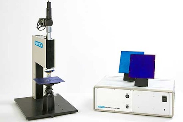
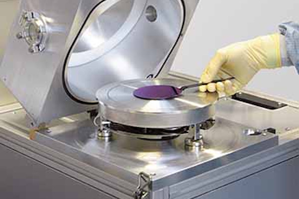
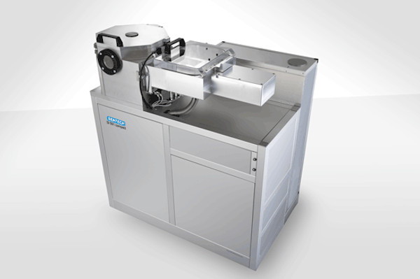
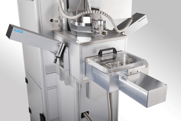
SENTECH Instruments of Berlin Germany develop and manufacture equipment for the processing and characterisation of SiC, combining precision plasma process systems with advanced optical metrology. Their article Processing Silicon Carbide (SiC), Understanding the Challenges and Finding Pathways to Precision expands on the subjects already outlined here with particular focus on how their technology can support scientists working with SiC.
The full article can be viewed here – https://sentech.com/news/processing-silicon-carbide-sic-understanding-the-challenges-and-finding-pathways-to-precision/
Explore our range of SENTECH Thin Film Metrology tools here.
Explore our range of SENTECH Plama Processing tools here.
