Precision at the Atomic Scale
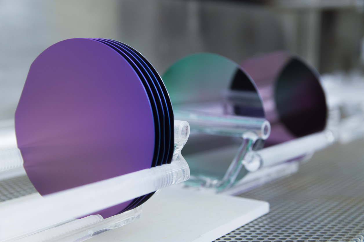
In the ever-evolving world of nanotechnology, precision is everything. From semiconductor manufacturing to biomedical coatings, the ability to deposit ultra-thin films with atomic-level control has transformed industries. This is where Atomic Layer Deposition (ALD) shines. First conceptualized in the 1970s, ALD has rapidly become an indispensable technique for developing nanostructured materials with unmatched uniformity, conformality, and precision.
Layer by Layer: A Brief History of ALD
The origins of ALD can be traced back to the 1960s and 1970s, when two independent research efforts – one in Finland by Tuomo Suntola and another in the Soviet Union by Valentin B. Aleskovsky – laid the foundation for the technique. Suntola’s work led to the first practical application of ALD in 1974 for the production of thin-film electroluminescent displays. Since then, ALD has grown into a cornerstone technology for advanced material fabrication.
“The beauty of ALD lies in its fundamental simplicity—layer by layer, atoms are placed with precision.”
Tuomo Suntola
What actually is ALD?
ALD is a thin-film deposition technique that relies on sequential, self-limiting surface reactions. Unlike conventional deposition methods, ALD enables:
- Angstrom-level thickness control for highly precise coatings.
- Superior uniformity across complex three-dimensional structures.
- Exceptional conformality, even on high-aspect-ratio surfaces.
By leveraging these properties, ALD has become a cornerstone of modern nanofabrication and plays a crucial role in:
- Semiconductor Scaling: ALD is essential for creating ultra-thin gate oxides and high-k dielectrics in next-generation transistors.
- Energy Storage & Conversion: The technology enhances battery electrode coatings and improves the efficiency of solar cells.
- Biomedical Coatings: ALD enables biocompatible and corrosion-resistant coatings for implants and medical devices.
- Optoelectronics: Advanced displays, LEDs, and photonic devices benefit from ALD’s ability to tailor optical and electronic properties.
How does ALD work?
ALD is based on self-limiting surface reactions which means that each step of the process will continue until every available reactive site on a surface has reacted. This ensures that each cycle deposits exactly one atomic layer.
Step 1:
- The first chemical (precursor A) is introduced into a reaction chamber along with a sample wafer
- The chemical reacts with the surface of the wafer to form a monolayer
- Once all reactive sites are occupied the reaction will stop, hence the term self-limiting
- Excess precursor and byproducts are then purged from the chamber using an inert gas
Step 2:
- The second chemical (precursor B) is introduced. This is often a reactant like water or ozone)
- It reacts with the layer formed by precursor A and completes the desired material layer
- Again this is self-limiting and will stop when all reactions have finished
- Excess precursor B and byproducts are purged.
Step 3:
- Repeat
- One atomic layer is added per cycle
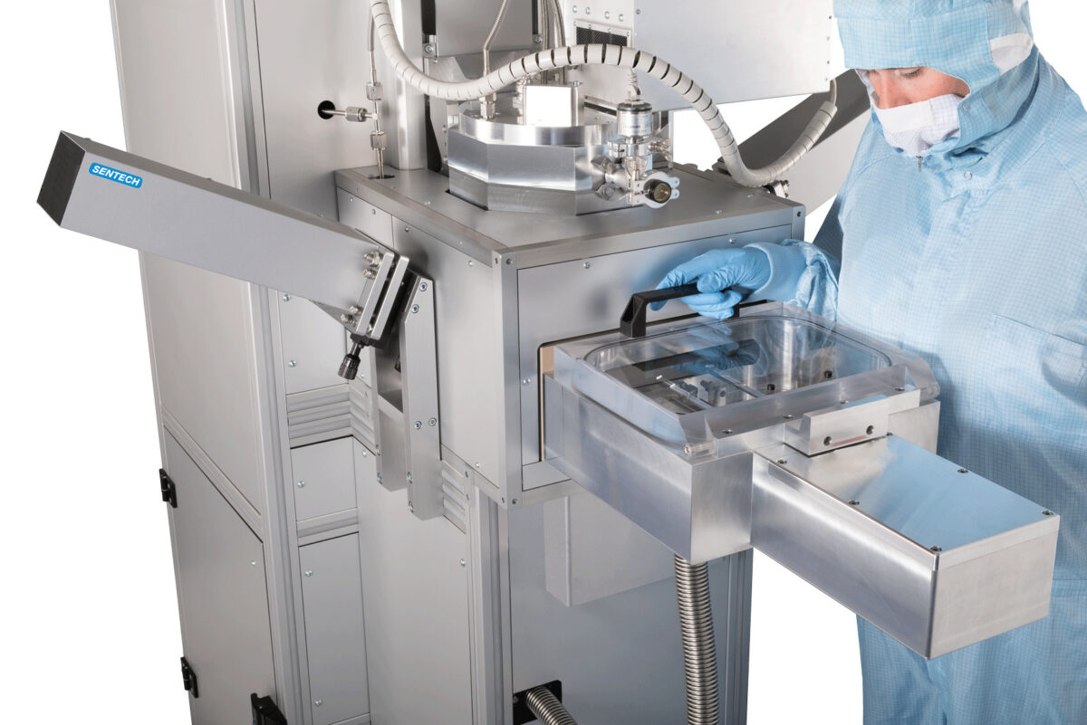
Mi-Net offers state-of-the-art ALD systems from SENTECH Instrument GmbH tailored for research and industrial applications.
Our product line features:
- Thermal ALD Systems: Ideal for high-precision oxide and nitride coatings.
- Plasma-Enhanced ALD (PEALD): Enables lower-temperature deposition for delicate substrates.
- Customizable ALD Solutions: Designed to meet the needs of cutting-edge nanostructuring applications.
Explore our full range of ALD solutions here: Mi-Net ALD Products.