A Spark of Innovation – From Lightning to Lab Coatings
Did you know that the same type of plasma found in lightning bolts is also used in some of the most cutting-edge materials science labs? While lightning releases an immense burst of energy in nature, in the lab, plasma is harnessed with precision to enable advanced surface engineering. Nowhere is this more evident than in the field of thin film processing, where plasma-based deposition techniques are helping researchers and engineers create coatings with unparalleled precision, uniformity, and performance.
A Brief History of Plasma Deposition
The roots of plasma deposition stretch back to the early 20th century, when Nobel Prize-winning chemist Irving Langmuir coined the term “plasma” to describe the behaviour of ionised gases in electrical discharges. It wasn’t until the 1960s and 70s, however, that plasma began to be used in materials processing.
The development of Plasma-Enhanced Chemical Vapour Deposition (PECVD) was driven by the need for lower-temperature deposition techniques suitable for fragile semiconductor materials. Scientists discovered that introducing RF (radio frequency) energy into a low-pressure gas environment created plasma that could trigger surface reactions, enabling the formation of thin films without high heat.
This innovation paved the way for modern Plasma-Enhanced ALD (PEALD), which combines the precision of atomic layer deposition with the reactive energy of plasma for ultra-thin, high-performance coatings.
“Plasma is a fourth state of matter—but in thin films, it’s the first state of innovation.”
What is Plasma Deposition?
Plasma deposition is a technique that uses plasma to deposit thin films onto substrates. It’s commonly used in microelectronics, optics, and materials science to fabricate films with controlled thickness, chemical composition, and physical properties.
PECVD and PEALD, two prominent plasma-based techniques, are game-changers because they allow deposition at lower temperatures than conventional techniques—making them ideal for use with temperature-sensitive materials and substrates.
In PECVD, plasma is used to energise precursor gases, enabling chemical reactions at the surface of the substrate. This results in the formation of a solid film with excellent conformality and adhesion. Recent innovations have focused on improving:
- Deposition rate – achieving faster throughput without compromising quality.
- Film density and uniformity – critical for high-performance electronics.
- Process flexibility – accommodating a wider range of materials and complex geometries.
PEALD combines the atomic-level control of ALD with the enhanced reactivity of plasma. This hybrid approach enables:
- Superior step coverage on high-aspect-ratio structures.
- Lower temperature processing, crucial for sensitive substrates like polymers or complex multilayer devices.
- Tailored film properties, including improved hardness, chemical resistance, and dielectric performance.
Recent breakthroughs in Inductively Coupled Plasma (ICP) PECVD and ALD systems have further expanded the capabilities of plasma-based deposition. These systems enable highly reactive plasma environments while minimising ion bombardment at the substrate—ideal for precise, high-purity film growth.
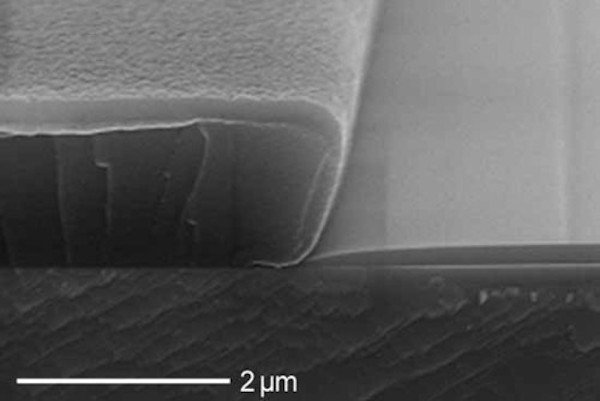
Accuracy and Repeatability for Thin Film Metrology
Plasma-based deposition techniques support this by producing films with:
- High uniformity across large substrates.
- Reproducible thickness control at the nanometre scale.
- Improved interface quality, which enhances measurement accuracy in ellipsometry, reflectometry, and X-ray metrology.
These qualities are particularly important in fields like semiconductor manufacturing, advanced optics, and photonics, where even the slightest inconsistency can lead to performance losses.
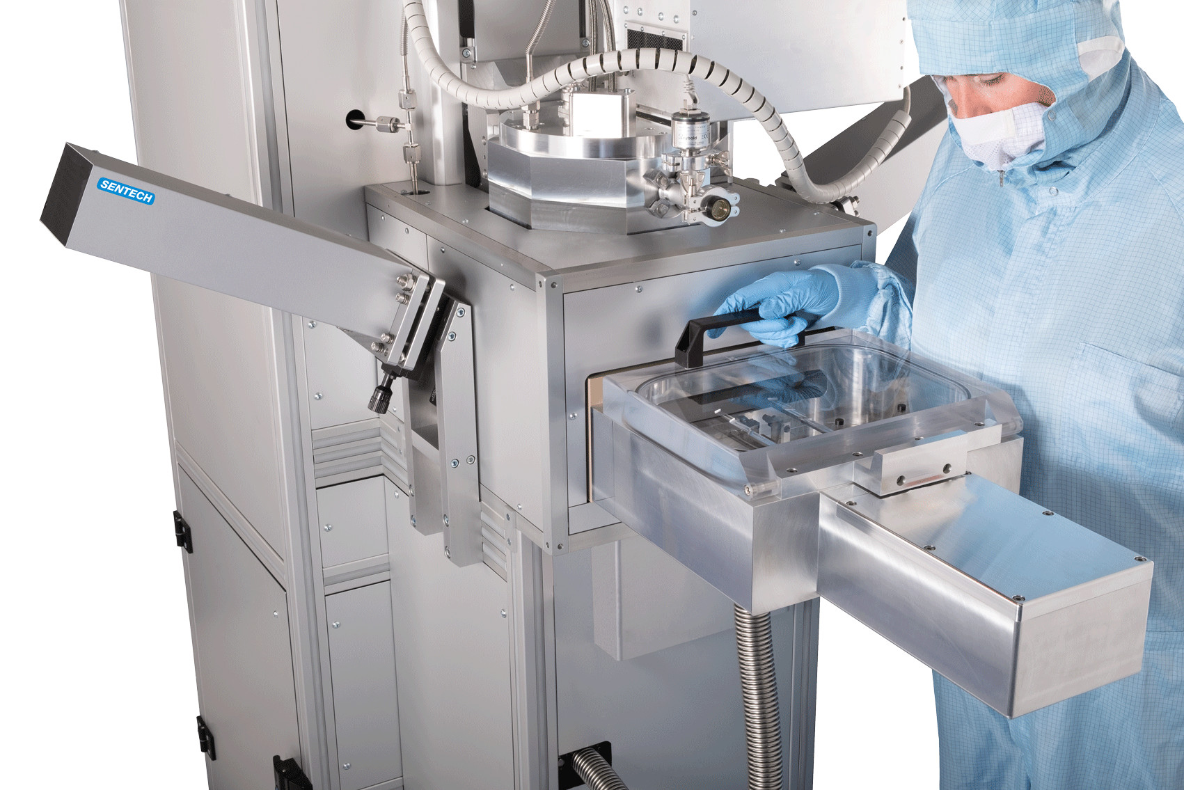
At Mi-Net, we offer a range of cutting-edge plasma deposition systems, including advanced IPECVD and Plasma-Enhanced ALD platforms designed for both research and industrial-scale applications. Our solutions are built for:
You can explore our full range of thin film processing systems here: Mi-Net Plasma Deposition.
Looking Ahead: Plasma’s Role in the Future of Materials Science
As devices continue to shrink and material complexity increases, plasma deposition techniques will remain at the forefront of thin film innovation. From ultra-thin coatings for flexible electronics to advanced passivation layers for quantum devices, plasma processes are shaping the next generation of technology—one atomic layer at a time.