When it comes to the performance and reliability of materials, the devil is often in the detail. And those details lie on the surface. Understanding this is crucial for many situations – when it comes to the precise layering of wafers for microchips, for example, or quality controlling medical devices (e.g., stents, prosthetics). When it comes to measuring surface roughness for aerodynamics and fuel-efficiency or ensuring that optics surfaces are free of defects. Surface profilometry is a critical tool in material science, which allows researchers and manufacturers to assess the topography of a material with exceptional precision. From nanoscale roughness to large-scale surface features, profilometry provides insights that are essential for material characterisation and quality control. We explain more in our latest insights blog.
Surface profilometry is a technique used to measure the texture, roughness, and contour of a surface. By analysing these parameters, scientists can determine how a material will behave in real-world applications, like assessing the wear resistance of an automotive component. The data generated by profilometry helps optimise manufacturing processes and ensures compliance with stringent quality standards.
The earliest profilometers were mechanical devices that physically traced a surface with a stylus. While effective, these tools were limited by their resolution and speed. Today, advanced optical profilometers have revolutionised the field, providing nanometre-scale precision and rapid measurements.
Surface profilometry has a wide range of applications across industries.
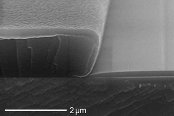
- Semiconductor Manufacturing: Profilometry ensures the smoothness and uniformity of wafers, enabling the precise layering of materials essential for microchips.
- Medical Devices: The surface characteristics of implants, such as stents and prosthetics, are crucial for biocompatibility and long-term performance.
- Aerospace and Automotive: Surface roughness can affect aerodynamics and fuel efficiency. Profilometry helps optimise surface finishes to meet these exacting demands.
- Optics and Photonics: High-precision optics require surfaces free from defects. Profilometry ensures that lenses, mirrors, and coatings meet the required specifications.
Surface profilometry plays a pivotal role in quality control.
- Detecting Defects: Profilometry can identify surface imperfections that may compromise a product’s performance or lifespan.
- Verifying Tolerances: Measuring surface roughness and texture ensures that materials meet strict industry standards.
- Optimising Processes: By analysing surface data, manufacturers can refine production techniques to achieve better consistency and efficiency.
As industries continue to demand greater precision, the field of surface profilometry is evolving rapidly.
- AI Integration: Artificial intelligence is being used to interpret surface data more effectively, identifying patterns and anomalies with greater speed.
- Nanometre Precision: Advanced technologies are enabling the measurement of even the smallest surface features, essential for applications like nanotechnology and quantum devices.
- In-Situ Measurements: Real-time surface measurements during manufacturing processes are becoming increasingly common, allowing for immediate adjustments and reduced waste.
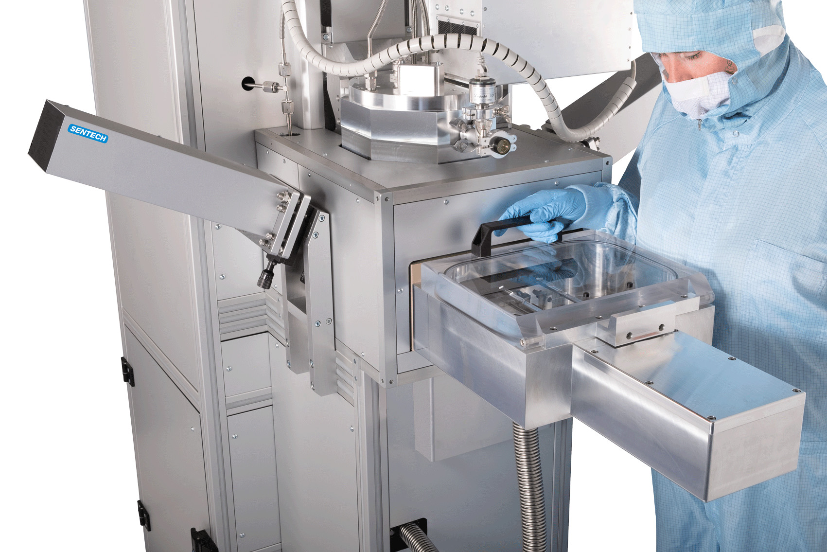
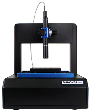
Nanovea, a global leader in metrology solutions, offers cutting-edge tools that set new standards in surface profilometry. Their PS50 profilometer, available through Mi-Net Technology, combines versatility with unparalleled accuracy. The PS50 can perform non-contact measurements, and what sets Nanovea’s profilometers apart is their ability to measure a wide variety of different material types and sizes with minimal training, allowing users to visualise surface features in extraordinary detail . With advanced software capabilities, the PS50 enables automated measurements, data analysis, and reporting, streamlining workflows and enhancing productivity.
Surface profilometry is more than just a measurement technique; it’s a gateway to understanding and optimising material performance. Tools like the Nanovea PS50 profilometer exemplify the cutting-edge technology driving this field forward, offering unparalleled insights that empower researchers and manufacturers alike. From semiconductors to medical devices, surface profilometry ensures that the materials we rely on meet the highest standards of quality and performance.
So, the next time you hold a flawlessly smooth gadget or marvel at a precision-engineered component, remember the science behind the surface. Surface profilometry may be behind the scenes, but its impact is felt in every corner of modern life.