Nanoindentation has become a widely applied technique for measuring mechanical behaviours of materials at small scales. The high-resolution load-displacement curves from the nanoindentation measurement can provide a variety of physicomechanical properties including hardness, Young’s modulus, creeping, fracture toughness and many others.
One significant bottleneck for further popularisation of the nanoindentation technique is time consumption. A mechanical property mapping by conventional nanoindentation procedure can easily take hours so this hinders the application of the technique in the mass production industries, such as semiconductor, aerospace, MEMS and many others.
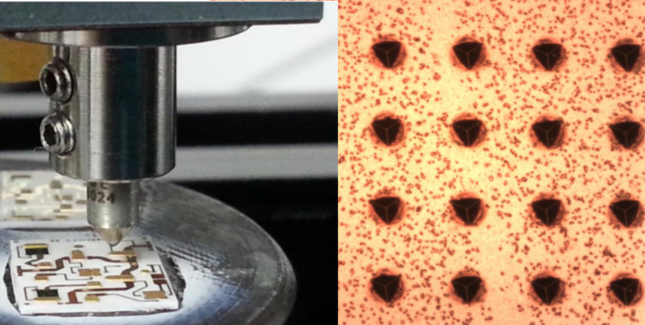
In this application note Nanovea demonstrate their mechanical tester in fastmap mode to map the mechanical property of a circuit board at high speed and importantly with high precision and reproducibility.