Thin films are everywhere. They are a layer of material that ranges from fractions of a nanometre to a few micrometres in thickness. They can be found in everything from optical devices to electrical components to protective coatings – wherever a very thin layer of material is needed for a specific function.
But their incredible role often goes unnoticed. Unsurprisingly they are extremely difficult to measure. Just imagine trying to measure a layer of material thousands of times thinner than a human hair. Fortunately, a host of scientific advancements are unlocking new possibilities for innovation across a range of industries. But with so many techniques out there, it can be a challenge to know which are most applicable to your business or research. In this article, we go through some of the latest developments in thin film metrology and the exciting ways they are being utilised.
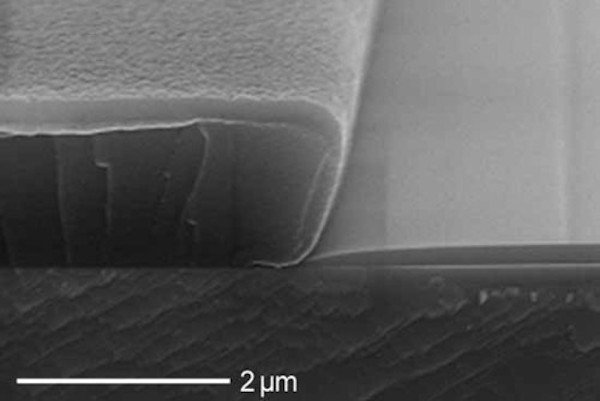
Let’s start with contact (mechanical) methods. Stylus profilometry, for example, works by using a physical stylus which drags across a film’s surface to measure height differences – measuring step height rather than absolution thickness. It is generally considered to be easy-to-use and cost-effective. Atomic Force Microscopy (AFM) uses a nanoscopic probe to scan the surface to measure height variations, providing high-resolution 3D surface profiling. It is well suited for films with rough or textured surfaces, and for measuring thickness at the nanoscale.
But the key challenge with contact methods is the requirement to measure the step of the film (from the substrate to the top of the film). That means in most cases you need to damage the film by cutting into it, or you must find an edge which is never straightforward. The advantage of optical (non-contact) methods is that you don’t need to touch or damage film and there’s no need for a step. Let’s focus on these in a bit more detail.
Optical (non-contact methods) include ellipsometry, reflectometry and optical profilometry.
- Ellipsometry was first pioneered by French physicist Paul Drude in the late 19th century. Drude’s work on polarised light interactions made ellipsometry a cornerstone of thin film metrology thanks to its precision and versatility – allowing for measurement of films through how light changes polarity when it reflects off the surface. Advancements in spectral range and modelling capabilities has led to spectroscopic ellipsometry – its non-destructive nature makes it valuable for industries including semiconductors and photovoltaics. Take a physics lab studying organic photovoltaic (solar cell) layers, for example. Ellipsometry can be used to analyse thickness, uniformity, and optical properties.
- Reflectometry is similar but is more specifically used to measure how light or other waves reflect off a surface – to identify objects, spot anomalies and/or analyse surface properties. Advances in this space, particularly spectral reflectometry, have made this technique particularly useful when it comes to measuring thickness in real time, when speed and accuracy is essential.
- Optical profilometry involves using light to measure the topography of a surface, including roughness, defects, and other characteristics. The evolution of higher resolution imaging and faster data acquisition has allowed for more detailed surface mapping. As with stylus profilometry this does rely on the user finding or creating a step.
- X-Ray Reflectivity (measuring the intensity of x-rays from a flat surface) is a powerful tool for measuring density, thickness, and interface roughness in thin films. XRR uses X-ray diffraction to measure electron density changes between a film and a substrate, to determine thickness, roughness, and density. It is well suited to ultra-thin films (<10 nm), hard coatings, multilayers and semiconductor applications, and high-precision lab measurements.
The techniques have a range of applications.
- Semiconductors: As the demand for smaller and more efficient chips grows, thin film metrology ensures the precise deposition of materials essential for transistors, interconnects, and dielectrics.
- Optics and Photonics: High-performance optical coatings, such as anti-reflective and beam-splitting layers, require tight control over film thickness and refractive index.
- Renewable Energy: Thin film solar cells, including cadmium telluride and copper indium gallium selenide, rely on advanced metrology to optimise efficiency and durability.
- Medical Devices: Thin films used in biomedical implants, drug delivery systems, and diagnostic tools require precise characterisation to ensure performance and biocompatibility.
SENTECH is pioneering thin film metrology solutions.
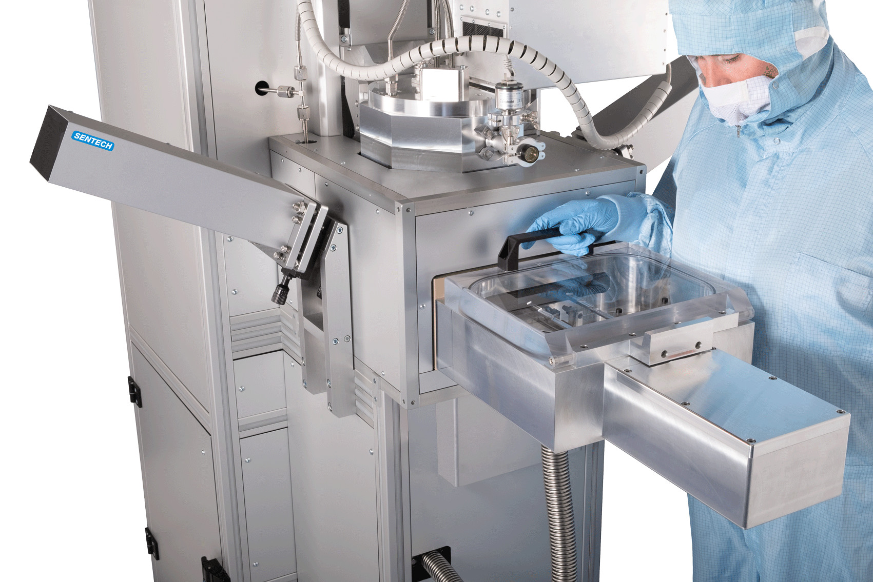
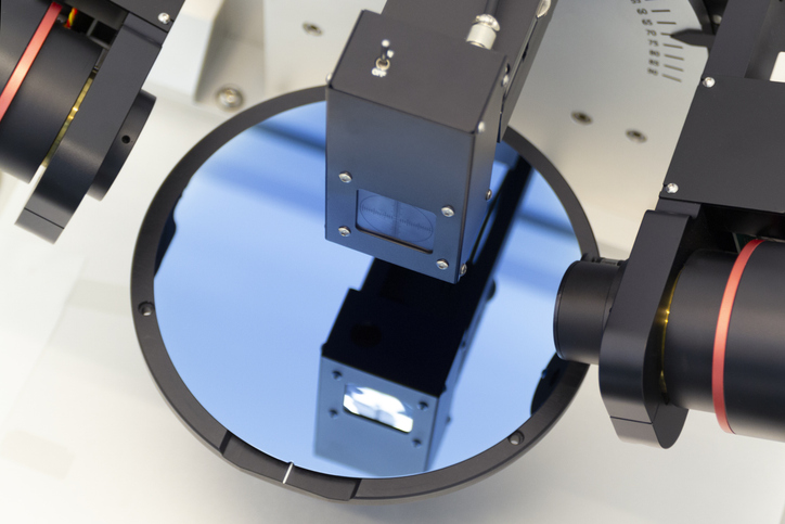
SENTECH Instruments offer a comprehensive range of tools designed to meet the evolving needs of these kind of applications. Their product portfolio includes state-of-the-art spectroscopic ellipsometers, such as the SENresearch 4.0 series, which deliver unparalleled accuracy in thin film characterisation. SENTECH’s reflectometers are ideal for high-throughput environments, combining speed with reliability. Their modular systems can be tailored to specific applications, ensuring compatibility with the unique requirements of different industries. The integration of advanced software enhances data analysis, providing users with actionable insights to optimise their processes. You can read more about SENTECH here.
The future of thin film metrology is bright.
The ability to characterise films’ thickness, refractive index, and uniformity, is only going to improve. These advancements are driven by a new hardware, enhanced algorithms and even the advent of artificial intelligence. AI is being leveraged to improve data interpretation and identify patterns that were previously undetectable, reducing errors and accelerating decision-making. In-Situ Monitoring, or real-time measurement, during the deposition process is becoming increasingly important for maintaining quality control and minimising waste.
Thin film metrology is a critical enabler of technological progress, ensuring the performance and reliability of products across diverse industries. With continuous advancements in techniques like ellipsometry and reflectometry, companies and universities are better equipped to tackle the challenges of modern manufacturing and research. SENTECH’s innovative solutions exemplify the future of thin film measurement, combining precision, flexibility, and efficiency to drive success in a competitive landscape.
So, the next time you marvel at a smartphone’s screen or a solar panel’s efficiency, remember – thin film metrology may work in the background, but its impact is far from superficial!