A comprehensive range of sputtering materials and sizes available
Micro machined components in strategic materials such as molybdenum, tantalum, titanium and niobium
Garnet crystals and substrates for epitaxy
J-GRAPHENE is ahigh quality, low defect graphene dispersion
Czochralski (Cz) and float zone (Fz) for a large range of semiconductor applications
Scratch, indentation and wear testing all on one tool at nano and micro load ranges
3D non-contact profilometers for collecting and analysing sample height data
Robust, modular, and powerful pin on disc tribometers
Advanced 3D optical measurement solutions for quality assurance in production
Non-contact technology measuring real time strength and direction of electrical currents
Reproducing the wear interaction between a surface and the human finger
Measurement of surface tension between liquids and solids
Determining thin film properties by change in polarisation of light
Measuring thin film properties by reflection
Tribology testing in ambient or tailored environments
Real life testing of finished products in respect of resistance to hand abrasion
Scratch & indentation for hardness, elastic modulus, adhesion, cohesion plus more
Gain a deeper understanding of your materials
Measure surface roughness, form, profile, finish plus more
Low damage plasma enhanced chemical vapour deposition
Low damage etching and nano structuring
Deposition of layers in the nanometer scale
Deposition of coatings by the vacuum evaporation technique
Deposition of coatings by the sputtering technique
The dispersion, mixing, pulverization or emulsification of materials
Scintillator materials grown in crystal form
Scintillator material in organic form
Materials for the measurement of radiation dose
Sapphire in sheet, tube, rod and component form
LiF, Quartz or SiO2, InSb, Si, Ge, PET, ADP, Beryl, TlAP, RbAP, KAP and CsAP
Bespoke leak testing systems for small or large parts
Superb optical stability and unsurpassed shock and vibration resistance
The performance of a penta prism with more control and wavelength transmission
Beam alignment where three or more optical axes are required
Two-mirror optical assembly arranged at a 90-degree angle
Ball mounted hollow retroreflectors
Reflects light back towards it’s source with minimal scattering
Powerful, easy to use and cost effective AI based image recognition
A comprehensive solution for laboratories using several types of microscope and profilometer
Benchmark technology for 2D and 3D surface texture analysis and metrology, seamlessly integrates with profilometers and other surface measuring equipment
Conductive coating on one side to prevent EMI/RFI
Plastic optical filter with broadband AR coating on both sides
Privacy Glass & Light Control Film


The SENDIRA infrared ellipsometer is specially designed to use FTIR. The table top instrument links to a commercial FTIR instrument to provide excellent precision and high resolution in the spectral range from 1.7µm – 25µm.
The spectroscopic ellipsometer is focussed on the vibrational spectroscopic analysis of thin layers.
Applications range from dielectric films, TCOs, semiconductors to organic layers, and the commercial FTIR is still available to perform general vibrational spectroscopy as well.
SENTECH Instruments of Berlin have been manufacturing tools for thin film metrology and thin film processing since 1990. They are a growing company with a reputation for high quality reliable equipment and excellent service. Their tools are used in applications such as semiconductors, microsystems, photovoltaics, nanotechnology and materials research.
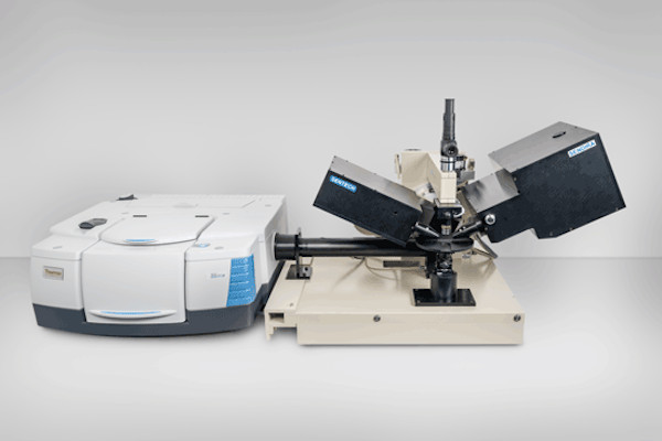
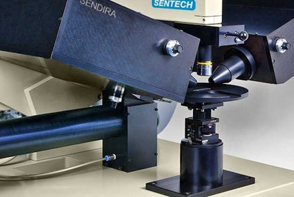
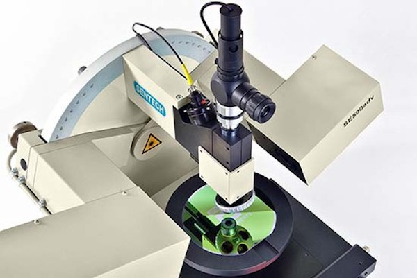
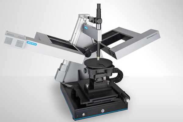
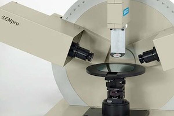
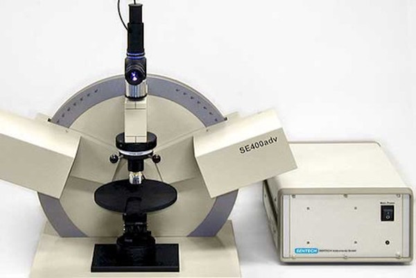
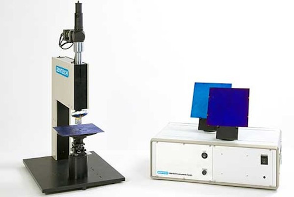
The SENTECH SENDIRA is focused on the vibrational spectroscopic analysis of thin layers. Applications include:
Vibrational ellipsometry
Combine two powerful methods – ellipsometry and vibrational spectroscopy to gain valuable insights into optical and vibrational properties of materials at a surface or interface.
Measurement of n and k
Reliable measurements to determine optical properties in the IR for IR optics. Draw meaningful conclusions, make predictions, and gain insights into the best layer and material designs for IR optics.
Identification of materials on opaque substrates
Allows you to explore the fundamental properties of matter in order to develop new materials for the advancement of cutting edge technologies.
Determination of crystal modification
To provide fundamental insights into the structure and properties of your chosen materials.
Composition analysis
To guide the synthesis and modification of your materials to meet desired performance criteria.
Determination of impurities
Accurate and precise measurement of impurities for reliability in your experimental results.
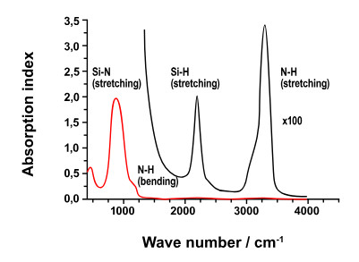
Orientation of organic molecule chains
Gain a crucial understanding of optical and spectroscopic orientation of molecules vital to many leading edge applications in lab-on-a-chip, lifescience and bio-sensor applications.
Measurement of bond orientation
Accurately measure electronic, optical, and structural properties to clearly determine functionality in your applications.
Conductivity of films
Gain valuable information about the quality and performance of your materials for precise conductivity measurements.
Doping profiles
Enabling precise measurement and understanding of charge carrier concentration and electrical conductivity.
SENTECH regularly document and publish work using their thin film metrology tools. We keep many of these resources on our website in the form of application notes or publications. These are a great way to learn more about what can be achieved with a Sentech tool.


Other instruments in the SENTECH thin film metrology range.
We’re here and ready to provide information and answers to your questions
©Mi-Net 2023. All Rights Reserved.
Website by Fifteen.co.uk